We have learnt during our Physics tuition class that a diode is simply a p-n junction semi-conductor, which permits only one direction of flow of current. A p-type semiconductor can be defined as a semiconductor that has holes only, which are positively charged. The n-type semiconductor, on the other hand, has negatively charged carriers or simply, electrons. A p-n junction is formed by fusing the n-type and p-type semiconductors together. Primarily, silicon is employed as a semiconductor material, while germanium, on the other hand, is also used in a lot of cases.
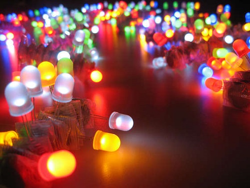
Diodes are manufactured based mostly on the function for which they are to be used. For instance, a zener diode operates in reverse biased mode and a varactor diode operates as a variable capacitor, hence their process of manufacturing is also different. A Light Emitting Diode (LED) is made such that, on recombination the electrons and holes discharge energy in form of light. Therefore, they are produced from materials such as; gallium phosphide, gallium arsenide, and so on, instead of using silicon, in order to have a larger potential barrier.
We will be required first to comprehend the V-I characteristics of a diode in order to understand how it operates. V-I characteristics is simply the voltage vs current graph plotted, showing the diode’s range of operation. A diode is basically a voltage controlled component. In a diode, the current flows in forward biased mode, whilst there is no charge flow in the reverse biased mode. A diode is in forward biased mode at the time when the battery’s negative terminal is connected to the diode’s n-terminal and the positive side of the battery to the p-terminal. As soon as voltage is applied to a forward biased diode, the diode doesn’t permit the flow of charge immediately. By increasing the voltage to a point known as the breakdown voltage, flow of current begins increasing and reaches its optimum. The breakdown voltage varies from one semiconductor material to another. In silicon, this breakdown voltage is seven volts. By applying the voltage, holes, which are positively charged, are repelled by the battery’s positive terminal and the electrons, which are negatively charged, are repelled by the battery’s negative terminal which leads to flow of charge. Hence the charge flows from the positive to the negative terminals.
Electrons and holes recombination occurs at the p-n junction and a narrow region is produced at the junction. This region comprises of majority carriers (holes in the n-layer) and minority carriers (electrons in the p-layer). This constrained region on the two sides of the junction is referred to as the “depletion region”. As soon as this region is formed, the flow of current becomes constant, practically. Additional voltage increase can destroy the diode by destroying the depletion region. When operating in the reverse biased mode, most diodes breakdown when the voltage is increased to a high level. When operating in reverse biased mode, practically, there is no charge flow initially. By increasing the voltage up to the reverse-threshold voltage, there is an indefinite increase of the current flow in reverse direction, leading to destruction of the diode.


